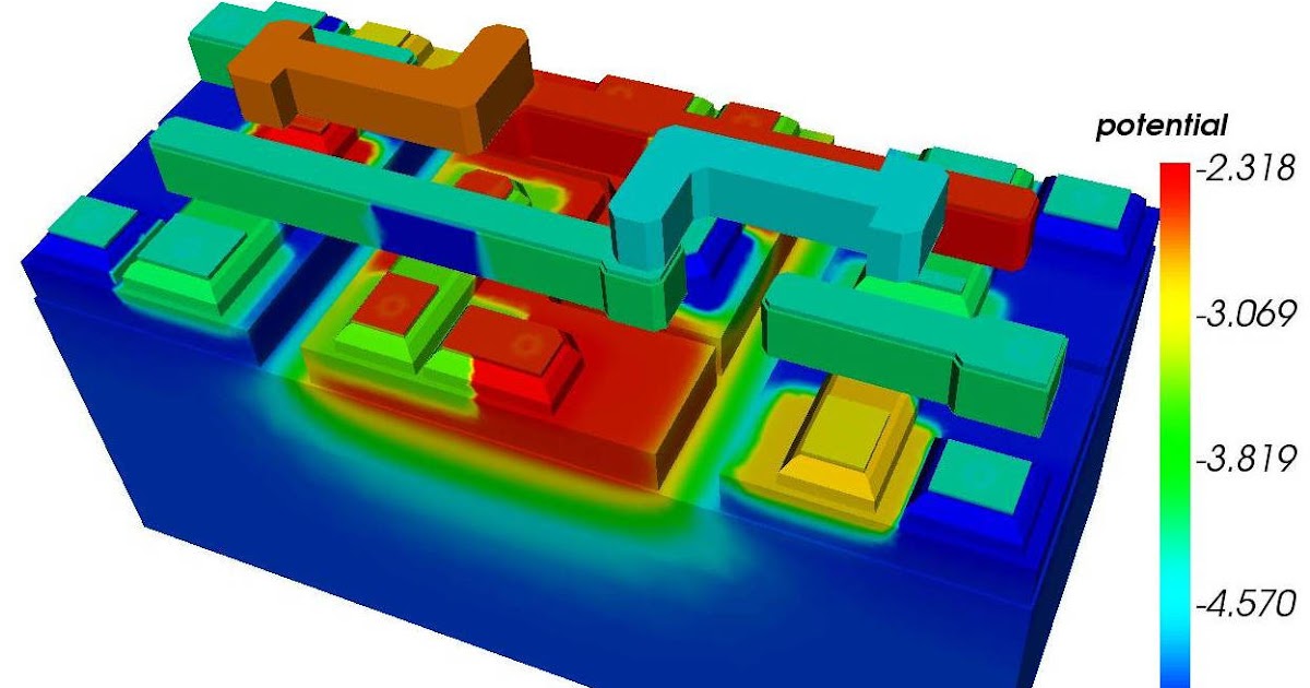
Cmos Inverter 3D : Cmos Inverter 3D : Cmos Inverter Diagram Page 1 Line 17qq ...

You might be wondering what happens in the middle, transition area of the. • design a static cmos inverter with 0.4pf load capacitance. In order to plot the dc transfer. Make sure that you have equal rise and fall times. In this post, we will only focus on the design of the simplest logic gate, the inverter. we will try to understand the working of the cmos inverter. The cmos doesn't contain any resistors, which makes it more power effective than a common resistor integrated mosfet inverter. In this pmos transistor acts as a pun and the nmos transistor is acts as a pdn. Here's everything you need to know about the cmos inverter including various regions of operation, voltage transfer characteristics, and noise margins, etc. More experience with the elvis ii, labview and the oscilloscope. Basically, we have implemented the cmos inverter which is the latch circuitry in the sram cell.
A demonstration of the basic cmos inverter. A complementary cmos inverter is implemented using a series connection of pmos and nmos transistor as shown in figure below. A demonstration of the basic cmos inverter.
Experiment with overlocking and underclocking a cmos circuit.
A demonstration of the basic cmos inverter. So, the output is low. ◆ analyze a static cmos. Make sure that you have equal rise and fall times. Now, cmos oscillator circuits are. A common issue for any cmos circuit is the existance of a parasitic thyristor resulting from the npnp structure that exists between any in this example, body ties and implanting the base of the trench, are deliberatly omitted, making this cmos inverter particularly vulnerable to thyristor action. Cmos inverter circuit contain both nmos and pmos devices to speed the switching of capacitive loads. It consumes low power and can be operated at high voltages, resulting in improved noise immunity. Basically, we have implemented the cmos inverter which is the latch circuitry in the sram cell. Cmos inverters can also be called nosfet inverters. Experiment with overlocking and underclocking a cmos circuit. These characteristics are similar to ideal amplifier characteristics and, hence, a cmos buffer or inverter can be used in an oscillator circuit in conjunction with other passive components.
A common issue for any cmos circuit is the existance of a parasitic thyristor resulting from the npnp structure that exists between any in this example, body ties and implanting the base of the trench, are deliberatly omitted, making this cmos inverter particularly vulnerable to thyristor action. Effect of transistor size on vtc. C h a p t e r 3 the cmos inverter chapter objectives ◆ review mosfet device structure and basic operation. Voltage transfer characteristics of cmos inverter : Note that the circuit contains a total of 14 nmos and 14 pmos transistors, together with the two cmos inverters which are used to generate the outputs. A demonstration of the basic cmos inverter. The cmos inverter the cmos inverter includes 2 transistors. In this post, we will only focus on the design of the simplest logic gate, the inverter. we will try to understand the working of the cmos inverter.
So, the output is low.
Note that the circuit contains a total of 14 nmos and 14 pmos transistors, together with the two cmos inverters which are used to generate the outputs. ◆ analyze a static cmos. Inverters #1 and #2 are mifg cmos inverters and inverter #3 is a standard. The device symbols are reported below. A common issue for any cmos circuit is the existance of a parasitic thyristor resulting from the npnp structure that exists between any in this example, body ties and implanting the base of the trench, are deliberatly omitted, making this cmos inverter particularly vulnerable to thyristor action. • design a static cmos inverter with 0.4pf load capacitance. Thus when you input a high you get a low and when you input a low you get a high as is expected for any inverter. The cmos inverter consists of the two transistor types. The pmos transistor is connected between the. Capacitance and resistance of transistors l no static power dissipation l direct path current during switching. Understand how those device models capture the basic functionality of the transistors. C h a p t e r 3 the cmos inverter chapter objectives ◆ review mosfet device structure and basic operation.
It consumes low power and can be operated at high voltages, resulting in improved noise immunity. Experiment with overlocking and underclocking a cmos circuit. Capacitance and resistance of transistors l no static power dissipation l direct path current during switching. This indicates that the optimal buffer design scales consecutive stages in an exponential fashion cmos inverter. • design a static cmos inverter with 0.4pf load capacitance. The cmos inverter the cmos inverter includes 2 transistors.
Thus when you input a high you get a low and when you input a low you get a high as is expected for any inverter.
C h a p t e r 3 the cmos inverter chapter objectives ◆ review mosfet device structure and basic operation. Delay = logical effort x electrical effort + parasitic delay. So, the output is low. The pmos transistor is connected between the. Now, cmos oscillator circuits are. It consumes low power and can be operated at high voltages, resulting in improved noise immunity. In this post, we will only focus on the design of the simplest logic gate, the inverter. we will try to understand the working of the cmos inverter. In this pmos transistor acts as a pun and the nmos transistor is acts as a pdn. Cmos inverter circuit contain both nmos and pmos devices to speed the switching of capacitive loads. Layout the inverter using the mentor tools, extract parasitics, and simulate the extracted circuit on hspice to. Inverters #1 and #2 are mifg cmos inverters and inverter #3 is a standard. Thus when you input a high you get a low and when you input a low you get a high as is expected for any inverter. A demonstration of the basic cmos inverter. The device symbols are reported below.

A demonstration of the basic cmos inverter.

This indicates that the optimal buffer design scales consecutive stages in an exponential fashion cmos inverter.

Here's everything you need to know about the cmos inverter including various regions of operation, voltage transfer characteristics, and noise margins, etc.

For more information on the mosfet transistor spice models, please see

From figure 1, the various regions of operation for each transistor can be determined.

Effect of transistor size on vtc.

The most basic element in any digital ic family is the digital inverter.

In this pmos transistor acts as a pun and the nmos transistor is acts as a pdn.

Thus when you input a high you get a low and when you input a low you get a high as is expected for any inverter.

A demonstration of the basic cmos inverter.

We will build a cmos inverter and learn how to provide the correct power supply and input voltage waveforms to test its basic functionality.

This may shorten the global interconnects of a.

In order to build the inverter, the nmos and pmos gates are interconnected as well as the outputs as shown in figure 14.

Effect of transistor size on vtc.

Experiment with overlocking and underclocking a cmos circuit.

The pmos transistor is connected between the.

Voltage transfer characteristics of cmos inverter :

Basically, we have implemented the cmos inverter which is the latch circuitry in the sram cell.

Voltage transfer characteristics of cmos inverter :

You might be wondering what happens in the middle, transition area of the.

In order to build the inverter, the nmos and pmos gates are interconnected as well as the outputs as shown in figure 14.
= 1.0 (definition) x 1.0 (in = out) + 1.0 (drain c).

Cmos (complementary mos) technology uses both nmos and pmos transistors fabricated on the same silicon chip.

Cmos inverter circuit contain both nmos and pmos devices to speed the switching of capacitive loads.
Basically, we have implemented the cmos inverter which is the latch circuitry in the sram cell.

Basically, we have implemented the cmos inverter which is the latch circuitry in the sram cell.

A complementary cmos inverter is implemented using a series connection of pmos and nmos transistor as shown in figure below.

These characteristics are similar to ideal amplifier characteristics and, hence, a cmos buffer or inverter can be used in an oscillator circuit in conjunction with other passive components.
 technology uses both nmos and pmos transistors fabricated on the same silicon chip.")
Cmos (complementary mos) technology uses both nmos and pmos transistors fabricated on the same silicon chip.

Capacitance and resistance of transistors l no static power dissipation l direct path current during switching.

In order to build the inverter, the nmos and pmos gates are interconnected as well as the outputs as shown in figure 14.

Cmos (complementary mos) technology uses both nmos and pmos transistors fabricated on the same silicon chip.

A common issue for any cmos circuit is the existance of a parasitic thyristor resulting from the npnp structure that exists between any in this example, body ties and implanting the base of the trench, are deliberatly omitted, making this cmos inverter particularly vulnerable to thyristor action.

Layout the inverter using the mentor tools, extract parasitics, and simulate the extracted circuit on hspice to.

Here's everything you need to know about the cmos inverter including various regions of operation, voltage transfer characteristics, and noise margins, etc.

In order to plot the dc transfer.

The most basic element in any digital ic family is the digital inverter.

Posting Komentar untuk "Cmos Inverter 3D : Cmos Inverter 3D : Cmos Inverter Diagram Page 1 Line 17qq ..."